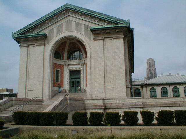
 Hamerschlag Hall
 MEMS wing

The Microelectromechanical Systems Laboratory is a facility for the design, analysis, modeling, fabrication, and characterization of MEMS devices. The MEMS Laboratory is housed in the Electrical and Computer Engineering Department in Hamerschlag Hall and is part of The Robotics Institute in the School of Computer Science. The MEMS group has access to several network-connected workstations and to several CAD tools. A Wentworth MP-901 probestation connected to a Kodak megapixel camera, precision manipulators, and an optical isolation table, and various test equipment is available for microelectromechanical device testing. We also use several CAD tools including MATLAB Simulink, Cadence and Saber simulators; and Ansoft Maxwell, MEMCAD, SDRC I-DEAS and ABAQUS finite-element packages. The MEMS Lab has access to a 3000 ft2, Class 100 cleanroom housing a variety of state-of-the-art semiconductor fabrication equipment. A new deep silicon reactive-ion etcher (STS) is presently installed in the cleanroom. In addition, a stand-alone XeF2 etcher (a gas-phase isotropic etchant of silicon) has been recently purchased as well as a new Dektak profilometer.
|
Hamerschlag Hall
|
MEMS wing
|